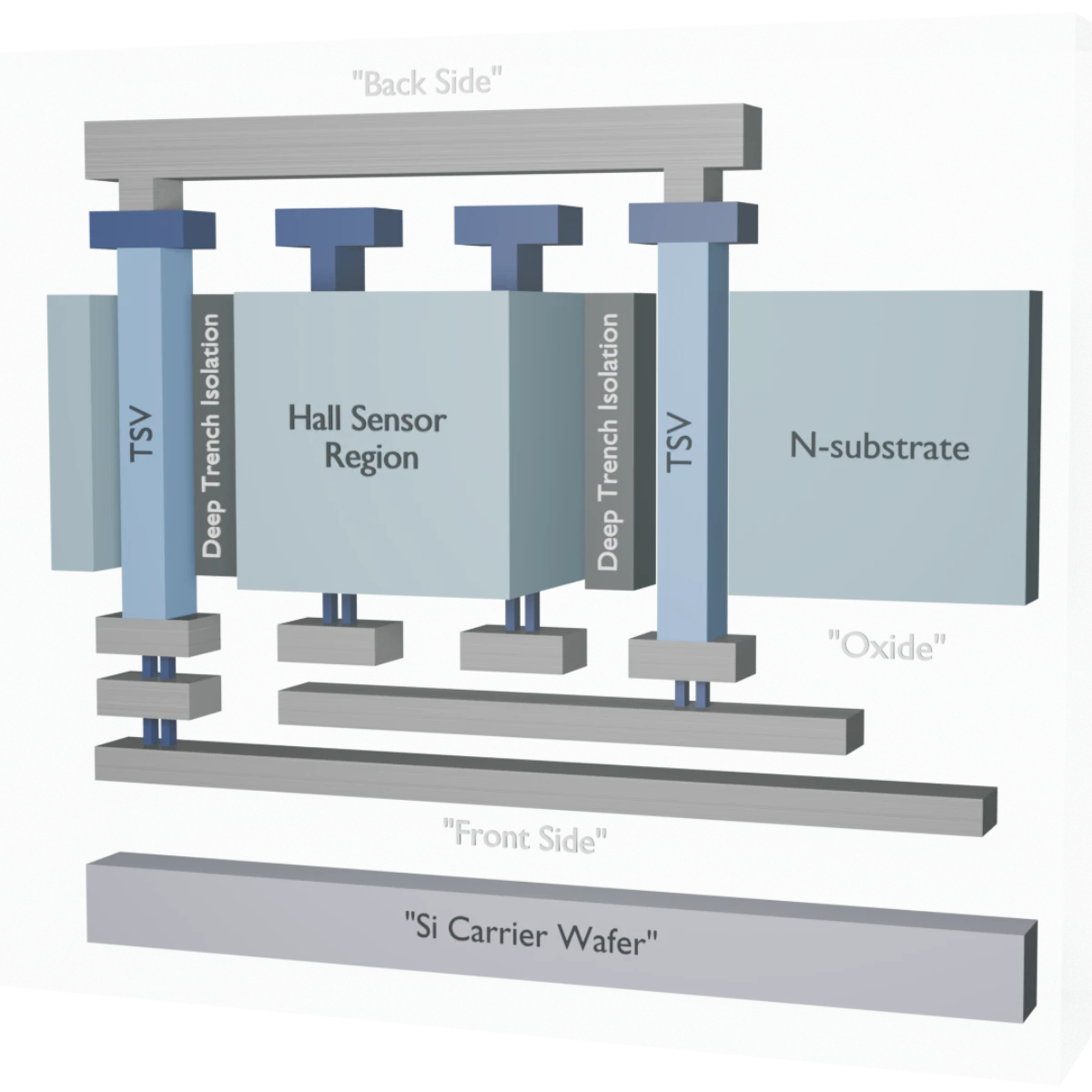
Our technology is what enables our sensors to offer high-performance and cost-efficient measurements of lateral magnetic fields. Our Hall-effect technology is based on patented true 3-dimensional Hall-effect technology.
This is enabled by our long-term experience in backside wafer processing. We use n++/n substrate with optimum epi concentration with no p-n junctions. Wafers are stacked using TSV bridge topology. Deep trench isolation enables full dielectric isolation of the Hall-effect. Our technology enables the stacking of logic wafers with sensor wafers and thus offers the highest possible integration density of a product.